|
|
|
| Photo Masks |
| |
|
| Download Ordering Information: Photo_Mask_Series.pdf |
| Introduction |
|
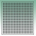
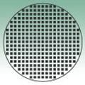
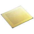
Masks are integral components in the lithographic process of semiconductor manufacturing. They contain transparent substrate which covered patterned opaque layer on it. This architecture used in lithography to block resist exposure in selected area and transfer circuit patterns from mask to wafer for mass prodcution.
We can providing 1x photomasks and 5x Wafer Stepper Reticles and others with Minium feature size (CD) of 0.1 micrometer. These photomasks are either direct-written on e-beam or laser systems or are manufactured from reticles using photorepeater system.
Tighter specifications and/or other plate sizes are available upon request. Contact us for more information to meet your needs.
|
|
| About Photomask Design |
|
Mask Fabrication Steps
The following is a process flow for typical mask manufacturing. After a mask file is received by a mask company, it uses either E-Beam/Laser lithography or Pattern Generator to make a mask prototype with one magnified die (normally from 5X to 10X), which is called reticle. Photolithography is then used to make an 1X original mask by repeat stepping the reticle. The original mask is named as master. Using masters, prints can be easily obtained by simple photolithography. Hence, prints are much less expensive than masters, but with compromised quality. In that prints which are produced from masters by photolithography, they are mirrored images to each other. In other words, one can't get both masters and prints in right images. One needs to specify the final product, which will have the right image.
Mask Material Issue, Soda Lime (SL) or Quartz?
Mask substrates can be made from a variety of materials, depending on applications. Coefficient of thermal expansion(CTE) of soda lime (9.4x10 -6 Deg C) is 20 times larger than that of quartz(0.5x10 -6 Deg C). If one worries about mask thermal expansion, quartz is a good choice. Further more, soda lime (SL) is fine and also much cheaper. Typically, anti-reflection chrome is chosen for the mask coating. Commonly speaking, when CD is bigger than 1 micron, soda lime is ok.
Mask Image Specification
Usually one mask contains many dies. One has to specify die size and step size for the die repeating, that is die array on the mask. There are two options for the array shape: square or truncated. If one chooses truncated, the die array will be cut according to the wafer shape, namely sphere. Otherwise, the die array will be a simple square. In case one mask has several layers, one has to provide name for each layer and number them. Depending on positive or negative photoresist one intends to use with the mask, he/she should specify the digitized area to be either CL (clear) or DK(dark). Digitized area normally represents the patterns on a mask. Field, where there is no pattern, is normally but not always complementary to the digitized area. For example, if you want a square pattern on the mask and define the digitized area to be DK, you will see the final mask with a black square with all other area transparent.
Mask companies should also be informed about the smallest feature size on the mask. This is defined by parameter critical dimension (CD). In the meantime, CD tolerance should be given. If the smallest feature is two micron, the CD tolerance will typically be +/- 0.25 micron for masters and +/- 0.5 micron for prints.
|
|
| Tone/Polarity and Orientation/Parity? |
|
Orientation/Parity
For a photomask layer, one side is coated with chrome, the other side without (glass only). We need to know which way round the mask has been designed, please specify one of the following when ordering
Reading: Right or Wrong Reading Chrome Down
The process determines how the design should appear. If you look at the mask on the chrome side (not through the glass) this is called "chrome up". If you look at the mask to the chrome through the glass, it is called "chrome down".
These appellations are used to specify whether the design is to be mirror imaged, i.e. "wrong reading" or look as it appears in the database, i.e. "right reading".
Polarity/Tone
We refer to our masks as Clear field / Dark field. This is the best way to describe if a mask is Positive or Negative. For example, Clearfield means that the data you have drawn in CAD will be Black/Opaque on the mask, with the background being clear. Dark field is obviously the opposite of this, where the items drawn on CAD will be clear and the background will be dark.
Sometimes, people use CD Tone instead of Clear field/ Dark field. The data you have drawn in CAD will be Black/Opaque on the mask means "CD Tone = DK", the items drawn on CAD will be clear means "CD Tone = CL".
|
|
| Tips for Photomask Design |
optimize your designs, we suggest the following:
1) avoid the use of acute angles (any angle less than 90-degrees),
2) avoid round or curved features, using straight-sided polygon edges instead,
3) avoid all but the simplest/squarest text fonts, using the fewest possible number of characters,
4) digitize the smallest areas possible (typically, this is the data, rather than the field).
Set gauge to control line/space to obtain excellent CD
Critical Dimensions (CDs, Minimum Feature Size)
Customers have very specific requirements for geometry sizes and specify certain geometry on the mask to be used as a gauge. These geometries are called critical dimensions or CDs. The customer indicates the target size or specifies of the CDs in microns (a thousand microns equals a millimeter) and the acceptable variance from that target (the CD Tolerance).
Examples of geometry used as CDs:
|
|
| Glossary |
|
Photomask: A glass substrate with a layer of chrome on one side. Some portion of chrome corresponding to an electronic circuit design is etched. Synonymous with mask, plate, mask layer
Critical Dimension: A geometry or space used as a gauge to monitor the pattern size and ensure that it is within the customer's specification: Abbreviated as CD. Synonymous with Minimum Feature Size
CD Tolerance: A plus/minus value that dictates the allowable disparity between each actual CD reading and a target value. The target value may be either an absolute or mean number.
CD Uniformity: A specified (often plus/minus) value that dictates the allowable difference between the lowest and highest CD values within a given set of readings. It can apply to either a mean or absolute value.
Clear: An area on the mask where the chrome has been removed and there is only glass.
Clear Field: The background area surrounding the component geometry is clear, that is, there is no chrome.
Dark: An area on the mask where the chrome has been not removed, i.e., the area is covered by chrome.
Dark Field: The background area surrounding the component geometry is chrome (dark).
Orientation: The relationship of the mask pattern to the original drawn pattern when looking through the mask substrate at the opaque layer. It may be correct (looks the same) or it may be mirrored (looks like the mirror image of the drawing).
Synonymous with Parity.
Parity: Whether an image is right reading or wrong reading (mirror image).
Synonymous with Orientation.
Polarity: the field tone, see clear field and dark field. Synonymous with CD Tone
CIF: An abbreviation for Caltech Intermediate Format, hierarchical pattern data format that is used for mask layout. This software is "public domain" meaning available for free without licensing fees.
GDSII: A common format for hierarchical design that can be easily converted into mask making formats.
Defect: A flaw affecting the geometry such as unwanted chrome, missing chrome, and dirt.
Particles: Any element of dust or debris on a photomask.
Defect Inspection: An inspection for defects using die to die, die to database or visual methods.
Geometry: Intended pattern imaged on the photomask.
Micron: A unit of measure equal to 1/1,000,000th of a meter, about 1000 times thinner than a human hair.
Patterns: Features that are imaged on the mask.
Pattern Offset: Used when the pattern is not centered on the mask.
Registration: The positioning of patterns on a layer to corresponding patterns on other layers within the same device or to a design grid.
Synonymous with metrology.
Reticle: A photomask with patterns that are stepped (repeated side by side) onto the wafer.
Die: Each complete pattern.
Reverse Tone: A process by which the polarity of a mask pattern is inverted such that chrome becomes clear and clear becomes chrome. Usually done through the job deck or off line on data processing software.
Step and Repeat: (Stepping) The repetitive exposing of a single image in different specified places on the wafer.
Stepping Distance: The distance between exposures of pattern in the X and Y axis on a mask.
Shrinking: see Scaling
Glass Type: the type of photomask's substrate. It is quartz or soda lime glass. If one cares about the change due to temperature varies, quartz is chosen.
Scale Factor: Used to increase or decrease the pattern size.
Scaling: Global reduction in chip size, also know as shrinking.
Sizing: The increasing or decreasing of line width without scaling through use of software.
|
|
| Download Ordering Information: Photo_Mask_Series.pdf |
|
| |
|

